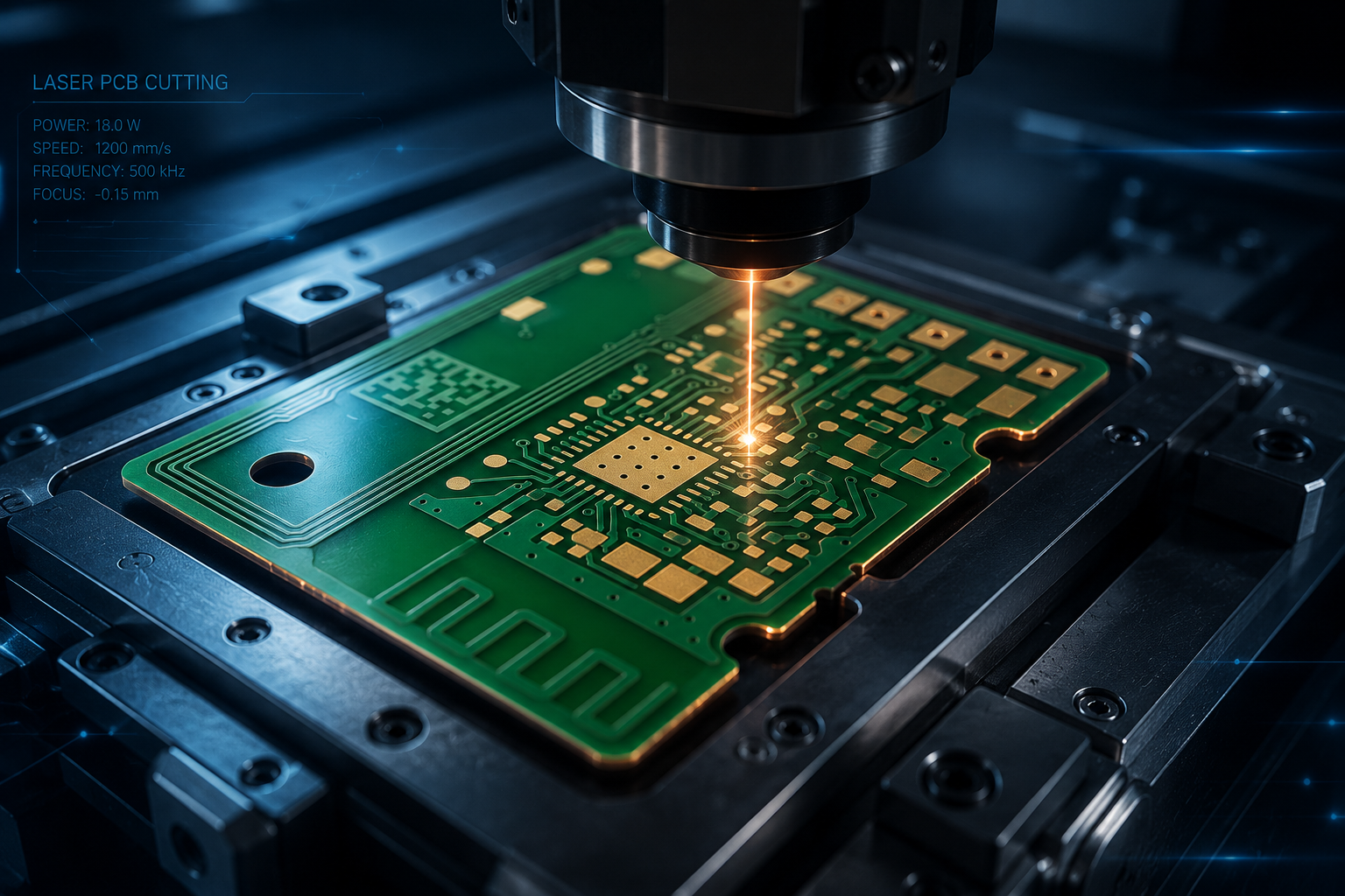
PCB Micromachining
PCB micromachining enables extremely precise, contact-free processing of printed circuit boards with micron-level accuracy. Laser technology creates fine features, micro-holes, isolation paths and complex geometries without mechanical stress, ensuring exceptional quality for advanced electronics manufacturing.
The Future of PCB Manufacturing Starts Here
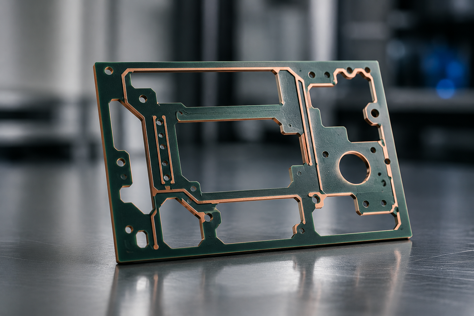
Micron-Level Precision
The laser operates with micron-level accuracy, enabling the production of ultra-fine traces, micro-holes, and complex geometries with outstanding precision and repeatability.

Contact-Free Processing
Because the process is completely non-contact, it eliminates mechanical forces, vibration, and material deformation, allowing even thin and delicate PCBs to be machined without damage.
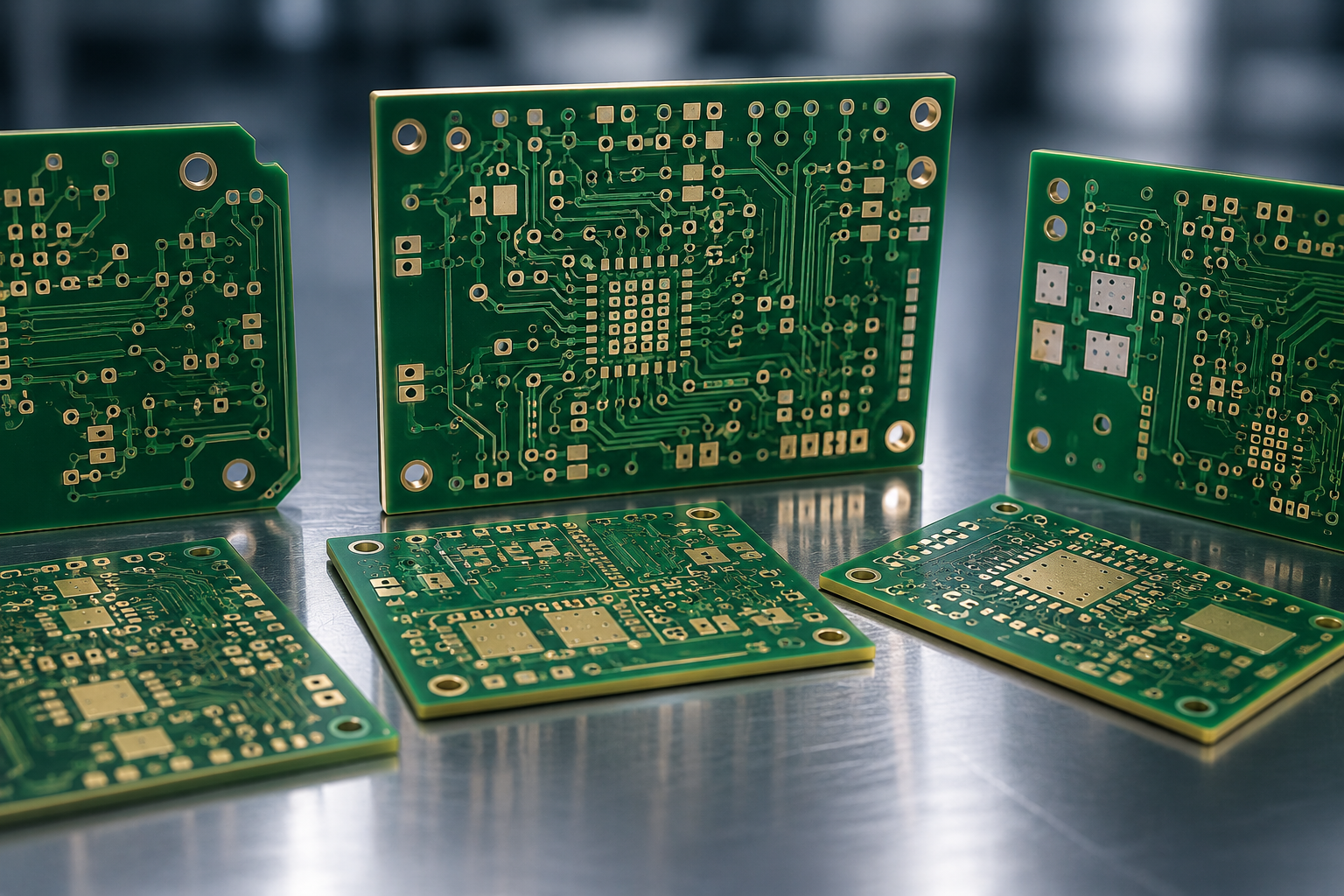
No Tool Wear
Since the laser beam is a non-contact tool, there is no tool wear. This ensures consistently high machining quality while eliminating tooling replacement costs and production downtime.
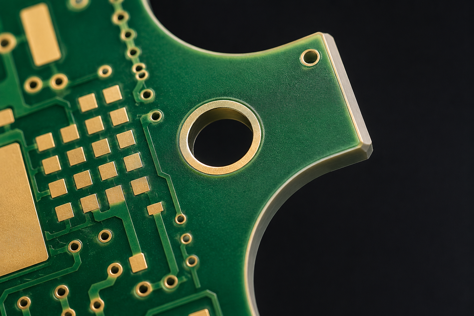
Burr-Free Results
Optimized laser parameters produce clean, burr-free edges with minimal post-processing, resulting in higher product quality and improved manufacturing efficiency.

Exceptional Repeatability
Every component is manufactured with the same high level of precision, making laser micromachining ideal for mass production and high-reliability electronic applications.

Complex Micro Features
Laser technology enables the creation of micro-holes, isolation channels, fine contours, intricate cut-outs, and high-density circuit structures that are difficult or impossible to achieve using conventional mechanical machining.
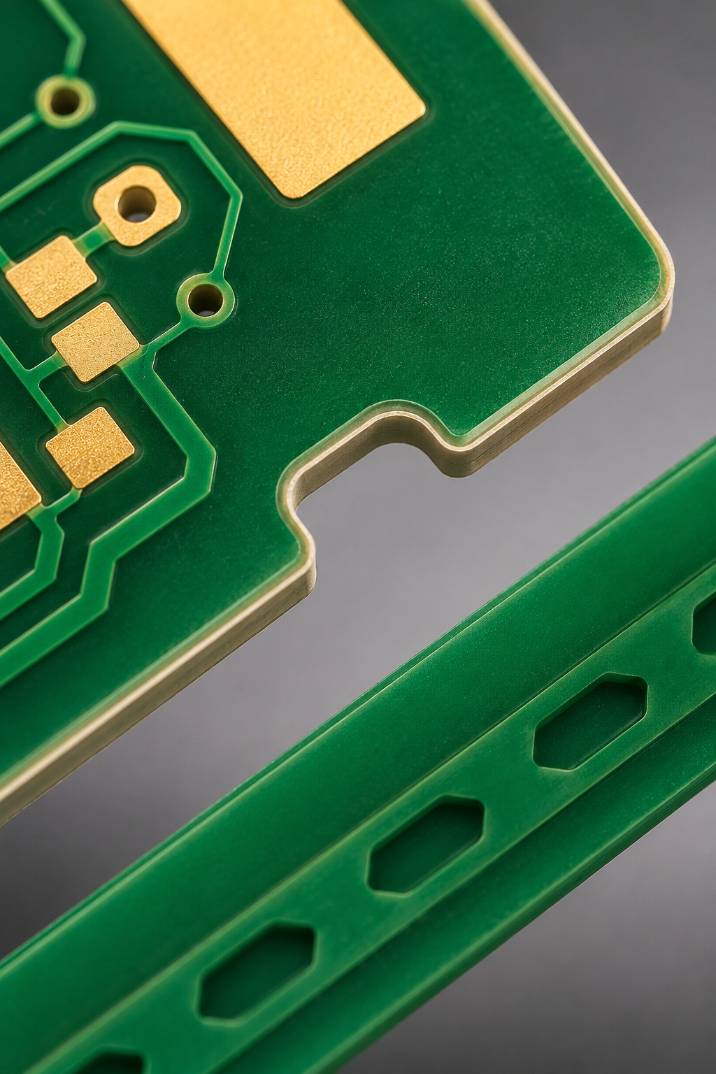
High-Speed Production
High-speed galvanometer scanning significantly reduces processing times while maintaining micron-level precision throughout the manufacturing process.
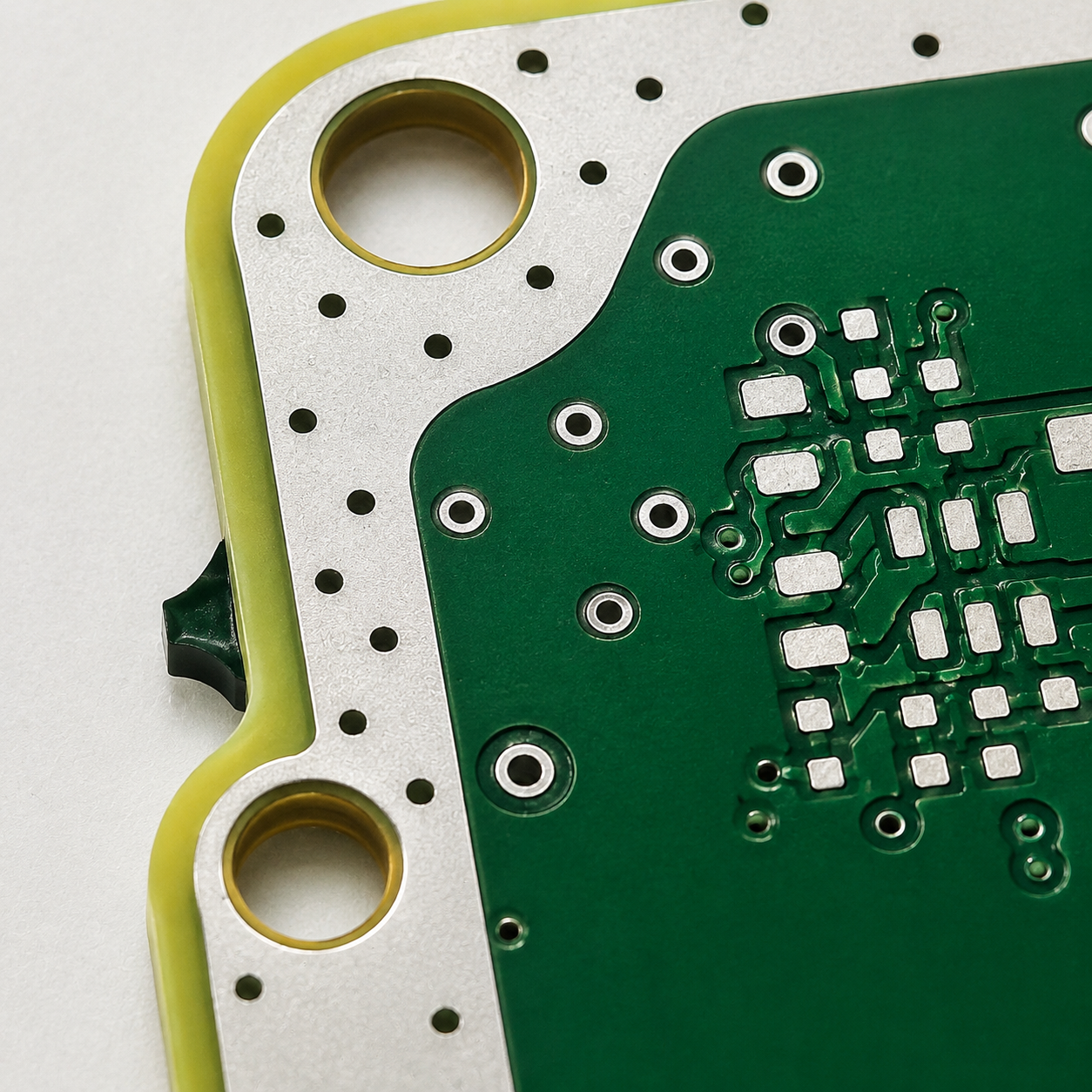
Minimal Heat-Affected Zone
The laser concentrates its energy into an extremely small area, minimizing heat input and protecting the surrounding material as well as delicate PCB structures from thermal damage.
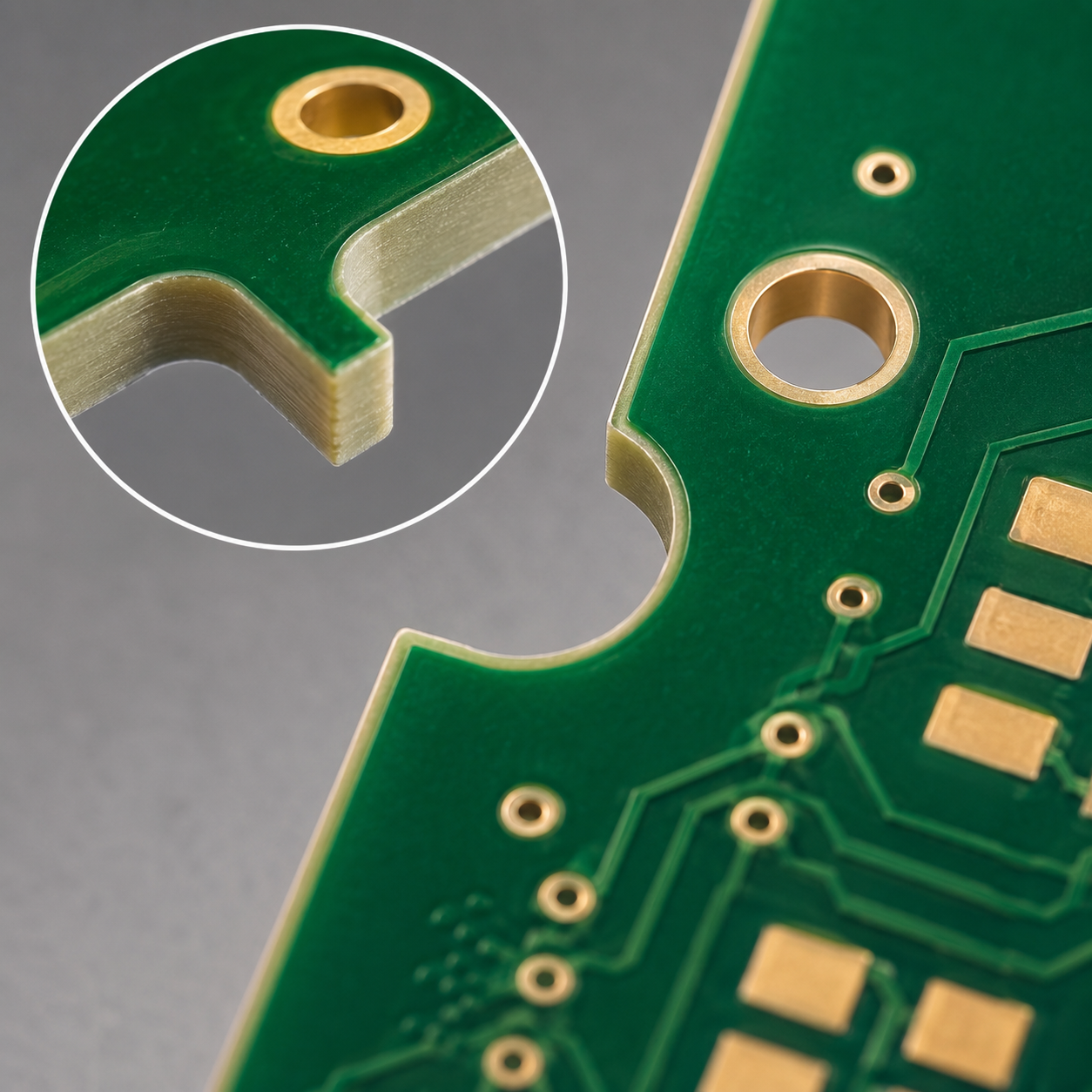
Consumable-Free Technology
No milling cutters, drill bits, or other consumable tools are required, resulting in lower operating costs, reduced maintenance, and increased production efficiency.
Laser PCB Milling vs. Conventional PCB Milling
Digital precision without mechanical tool wear.
Laser PCB milling combines ±0.01 mm positioning precision, scanning speeds of up to 14,000 mm/s and up to 100,000 hours of laser source lifetime with digitally programmable processing. Unlike conventional mechanical PCB milling, the laser process does not rely on a rotating cutting tool, enabling flexible geometry changes and highly automated production.
More Information| Aspect | Laser PCB Milling FibeerSX Laser Technology | Conventional PCB Milling Mechanical Router / Milling Tool |
|---|---|---|
| Positioning Precision | ±0.01 mm digitally controlled positioning | Machine-, spindle- and tool-dependent |
| Maximum Scan Speed | Up to 14,000 mm/s laser scanning speed | Limited by spindle speed, feed rate and cutting tool |
| Processing Method | ✓ Non-contact laser ablation | △ Mechanical material removal |
| Mechanical Tool Contact | ✓ None | — Direct tool contact |
| Cutting Tool Wear | ✓ No mechanical cutting tool | — Router bits wear during processing |
| Laser Source Lifetime | Up to 100,000 h laser source operating lifetime | Cutting tools require periodic replacement |
| Geometry Programming | ✓ Fully digital | CNC path + mechanical tool limitations |
| Process Changeover | ✓ Software / recipe based | Tool and setup changes may be required |
| Fine Structures | ✓ High precision feature size depends on optics, material and process | △ Limited by tool diameter |
| Small Internal Radii | ✓ Beam-based geometry | Minimum radius limited by milling-tool diameter |
| Mechanical Load on PCB | ✓ No cutting force | — Mechanical cutting forces |
| Sensitive / Thin Substrates | ✓ Suitable with optimized parameters | Mechanical loading must be considered |
| Material Selectivity | ✓ Parameter-controlled | Primarily depth / tool-path controlled |
| Depth Control | ✓ Digitally adjustable via energy, passes and process parameters | Mechanical Z-axis / tool-depth control |
| Consumable Cutting Tools | ✓ None | — Milling / router bits |
| Tool Replacement Downtime | ✓ No cutting-tool change | Periodic tool changes required |
| Process Repeatability | ✓ High stored digital process recipes | Influenced by tool wear, runout and mechanical condition |
| Dust / Debris | Process residue requires extraction | Mechanical chips and dust require extraction |
| Automation | ✓ Excellent | Good with CNC automation |
| Production-Line Integration | ✓ Direct inline integration | Possible with dedicated handling and milling station |
| Process Monitoring | ✓ Digital parameters | Machine and tool monitoring required |
| Traceability | ✓ Recipe & process data integration | Requires machine / production data integration |
| Design Flexibility | ✓ Geometry changed digitally | Tool diameter and mechanical access must be considered |


PCB Laser Cutting vs. Conventional Depaneling
Precision cutting without mechanical tool contact.
PCB laser cutting combines ±0.01 mm positioning precision, scanning speeds of up to 14,000 mm/s and digitally programmable cutting geometries with a non-contact process. Compared with V-scoring, CNC routing and punching, laser processing provides greater freedom for complex contours, rapid digital changeovers and automated production without mechanical cutting-tool wear.
More Information| Aspect | PCB Laser Cutting FibeerSX Laser Technology | V-Scoring Circular Blade Depaneling | CNC Routing Mechanical Milling | Punching Die / Punch Depaneling |
|---|---|---|---|---|
| Positioning Precision | ±0.01 mm digitally controlled positioning | Machine and blade dependent | Machine, spindle and tool dependent | Die and fixture dependent |
| Laser Scan Speed | Up to 14,000 mm/s scanning speed; cutting cycle depends on material and thickness | High throughput on straight score lines | Feed-rate dependent | Very fast per punching cycle |
| Process Type | ✓ Non-contact | △ Mechanical scoring | △ Mechanical routing | △ Mechanical punching |
| Mechanical Contact | ✓ None | Direct blade contact | Direct router-bit contact | Direct die / punch contact |
| Mechanical Stress on PCB | ✓ No cutting force | Mechanical stress during separation | Cutting forces and vibration | High localized mechanical force |
| Tool Wear | ✓ No mechanical cutting tool | Blade wear | Router-bit wear | Punch and die wear |
| Laser Source Lifetime | Up to 100,000 h laser source operating lifetime | Blades require periodic replacement | Milling tools require periodic replacement | Tooling requires maintenance and replacement |
| Geometry Freedom | ✓ Highly flexible digitally programmable cutting paths | — Primarily straight lines | ✓ Flexible contours | Geometry defined by tooling |
| Complex Contours | ✓ Excellent | — Very limited | ✓ Good | Requires dedicated die geometry |
| Small Internal Radii | ✓ Beam-based geometry | Not suitable for arbitrary internal contours | Limited by router-bit diameter | Defined by punch / die design |
| Design Change | ✓ Digital cutting path can be modified in software | Limited by scoring layout and machine setup | CNC program change; tooling may also change | New or modified tooling may be required |
| Product Changeover | ✓ Recipe / software based | Mechanical setup may be required | Program + tool / fixture setup | Die / punch change required |
| Dedicated Cutting Tool | ✓ None | Scoring blades | Router / milling bits | Product-specific punch / die |
| Prototype Production | ✓ Excellent no dedicated cutting tool required | Good for compatible straight-line layouts | Good | Less attractive when dedicated tooling is required |
| High-Mix Production | ✓ Excellent | Limited by panel geometry | Good | Multiple dies may be required |
| Large-Series Production | Highly automatable | Excellent for suitable straight-line panel layouts | Well suited | Excellent for stable, high-volume products |
| Process Repeatability | ✓ High digitally stored parameters and paths | Influenced by blade condition and setup | Influenced by tool wear and spindle condition | High with stable tooling and positioning |
| Mechanical Vibration | ✓ No cutting vibration | Mechanical forces present | Routing vibration present | Impact force present |
| Cutting Dust / Chips | Laser process residue requires extraction | Low compared with routing | Mechanical dust and chips generated | Limited cutting debris depending on material |
| Automation | ✓ Excellent | Excellent in dedicated production | Excellent | Excellent in dedicated production |
| Inline Integration | ✓ Direct integration | Possible | Possible with dedicated routing station | Possible with dedicated punching station |
| Process Data | ✓ Digital parameters | Additional monitoring may be required | CNC / machine data available | Additional monitoring may be required |
| Traceability | ✓ Recipe & process data | Requires production-data integration | Can be integrated with CNC production data | Requires production-data integration |
| Best Suited For | Complex geometries, high-mix production, precision depaneling and automated manufacturing | Straight-line PCB separation and high-volume production | Flexible mechanical contour routing | Stable geometry and very high production volumes |